What is Laser Photoplotting?
Laser photoplotting is a high-precision imaging process used to transfer digital design data (typically CAD or Gerber files) onto a photosensitive medium such as film or glass using a controlled laser beam.
At its core, a photoplotter is a computer-controlled machine that exposes extremely fine patterns onto photographic film. These patterns become the foundation for manufacturing processes like PCB fabrication, chemical etching, and microelectronics production.
Modern systems use laser-based raster imaging to achieve extremely fine resolutions—down to microns—ensuring that even the most intricate designs are accurately reproduced.
Key Characteristics:
- Ultra-high resolution (micron-level precision)
- Direct translation from CAD files to physical film
- Repeatable and scalable for production
- Suitable for complex geometries and fine line work
What are Photomasks (Phototools)
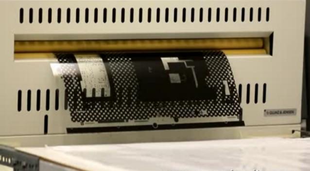
A photomask (also called a phototool) is a high-resolution transparency that contains the pattern of a design—typically made up of clear and opaque regions.
These masks act as stencils for light exposure, allowing selective transfer of patterns onto a material coated with photoresist.
How Photomasks Work:
- Clear areas allow light to pass through
- Opaque areas block light
- This creates a patterned exposure on the substrate
The result is a precise replication of the design onto the material, which can then be developed, etched, or processed further.
Laser Photoplotting vs Direct Imaging
| Feature | Laser Photoplotting | Direct Imaging (LDI) |
|---|---|---|
| Medium | Film or glass | Direct on substrate |
| Flexibility | High (reusable masks) | Moderate |
| Setup Cost | Low | Higher |
| Accuracy | Very high | Ultra-high |
| Use Case | Prototyping & production | High-end fabrication |
Laser photoplotting and photomasks form the backbone of modern precision manufacturing. By converting digital designs into high-resolution physical patterns, they enable accurate, scalable, and cost-effective production across industries.
Whether used for circuit boards, etched metal parts, or semiconductor devices, this technology ensures that even the smallest details are reproduced with absolute precision—making it an essential process in advanced manufacturing workflows.
Applications Across Industries
Laser photoplotting and photomasks are used in:
- Electronics (PCB manufacturing)
- Aerospace components
- Medical devices
- Automotive sensors
- Telecommunications hardware
- Microfabrication and MEMS
How Laser Photoplotting Creates Photomasks
Laser photoplotting is the primary method used to produce photomasks.
Step-by-Step Process:
- Design Creation
- Engineers create layouts using CAD software (e.g., PCB layouts)
- Data Conversion
- Files are converted into machine-readable formats (e.g., Gerber)
- Laser Imaging
- A photoplotter uses a laser to write the design onto film
- The laser exposes a photosensitive surface pixel by pixel
- Film Development
- The exposed film is chemically developed to reveal the pattern
- Registration & Alignment
- Holes or markers are added to ensure precise layer alignment
- Final Photomask
- The finished film becomes a usable photomask for manufacturing
This process ensures extreme accuracy and repeatability, especially for multi-layer designs.

Types of Photomasks
Positive Photomasks
- Clear pattern on opaque background
- Exposed areas become removed during processing
Negative Photomasks
- Opaque pattern on clear background
- Exposed areas remain after processing
The choice depends on the photoresist chemistry and manufacturing process.
How Photomasks Are Used in Manufacturing
Photomasks are essential in photolithography-based processes, where light is used to transfer patterns onto materials.
1. Printed Circuit Boards (PCBs)
- Each PCB layer uses a separate photomask
- UV light transfers copper trace patterns
- Enables precise electrical pathways
2. Chemical Etching
- Photomasks define areas to be etched or protected
- Used in metal parts, filters, and precision components
3. Semiconductor Manufacturing
- Photomasks define circuit patterns on silicon wafers
- Critical for microchips and integrated circuits
4. Glass and Optical Applications
- Used for:
- Calibration tools
- Reticles
- Micro-optics
Why Laser Photoplotting Matters
1. Precision & Resolution
Laser photoplotting can produce extremely fine features (microns level), critical for electronics and microfabrication.
2. Speed & Flexibility
Unlike traditional tooling, photomasks can be generated quickly from digital files, allowing:
-
Fast prototyping
-
Easy design updates
-
Reduced lead times
3. Cost Efficiency
Phototooling eliminates the need for expensive hard tooling, making it ideal for:
-
Low-volume production
-
Iterative design processes
4. High Repeatability
Ensures consistent output across:
-
Multiple production runs
-
Multi-layer assemblies
Request a Quote or Technical Consultation
Partner with a team that combines technical expertise with advanced imaging technology. Contact us today to discuss your photoplot or photomask requirements. Our experts provide guidance, solutions, and support to ensure your project achieves optimal accuracy and performance.